-
Edge AI with NSRAM
In this seminar, Prof. Mario Lanza presents the path towards deployment of artificial intelligence (AI) on the edge with Neuro-Synaptic Random Access Memory (NSRAM) cells. He also presents the advantages of this new device technology compared to threshold-type memristors for neuron applications.
-
Silicon neurons for AI
This talk was given by Prof. Mario Lanza during the 2025 Barcelona Artificial Intelligence Congress. He described how his team built ultra-compact silicon neurons using one single transistor, by operating it in punch-through impact ionization regime. The intro by the chairman is in Catalan, but the talk in English.
-
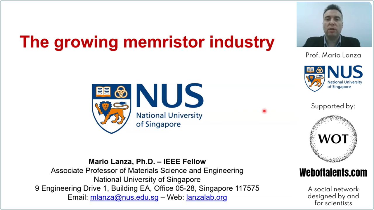
Beyond CMOS
This talk was given by Prof. Mario Lanza during an invited lecture at the Nanyang Technological University in 2025. He described the status of the memristor Industry, and how other materials and devices beyond the CMOS techonology could impact the semiconductor Industry.
-
2D materials
In this online seminar, Prof. Mario Lanza presents the fabrication of hybrid microchips by integrating two-dimensional (2D) materials a the back-end-of-line (BEOL) of silicon microchips, and he discusses their deployment in memristive applications for data storage, cmputation, encryption and communication.
-
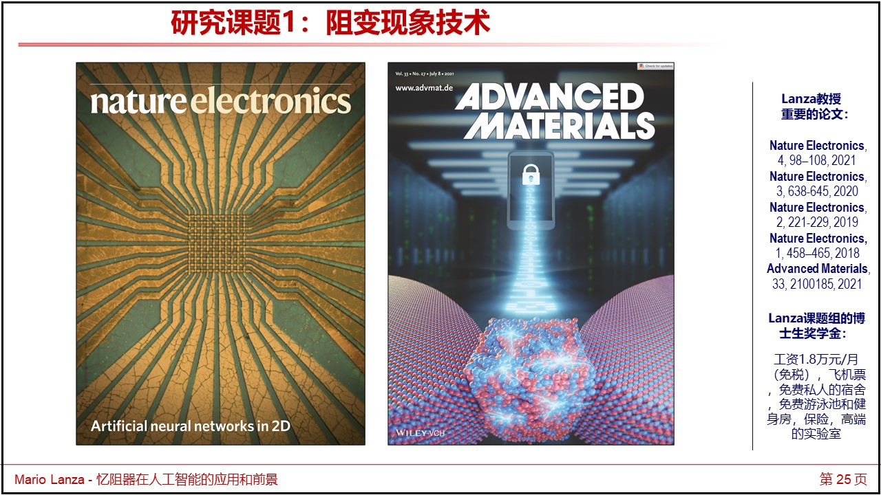
Memristors
In this online seminar, Prof. Mario Lanza speaks about the status of the memristor industry, discussing not only about device technology but also about market trends and commercial products. He also discusses the most rigorous methods to evaluate memristors and the future challenges to be solved.
-
Nanoelectronics
This talk was given in Chinese by Prof. Mario Lanza during the 7th International College Students '"Internet+" Innovation and Entrepreneurship Competition, which was attended by 15.8 million students. He presented his work and team for an audience at the Bachelor level.
-
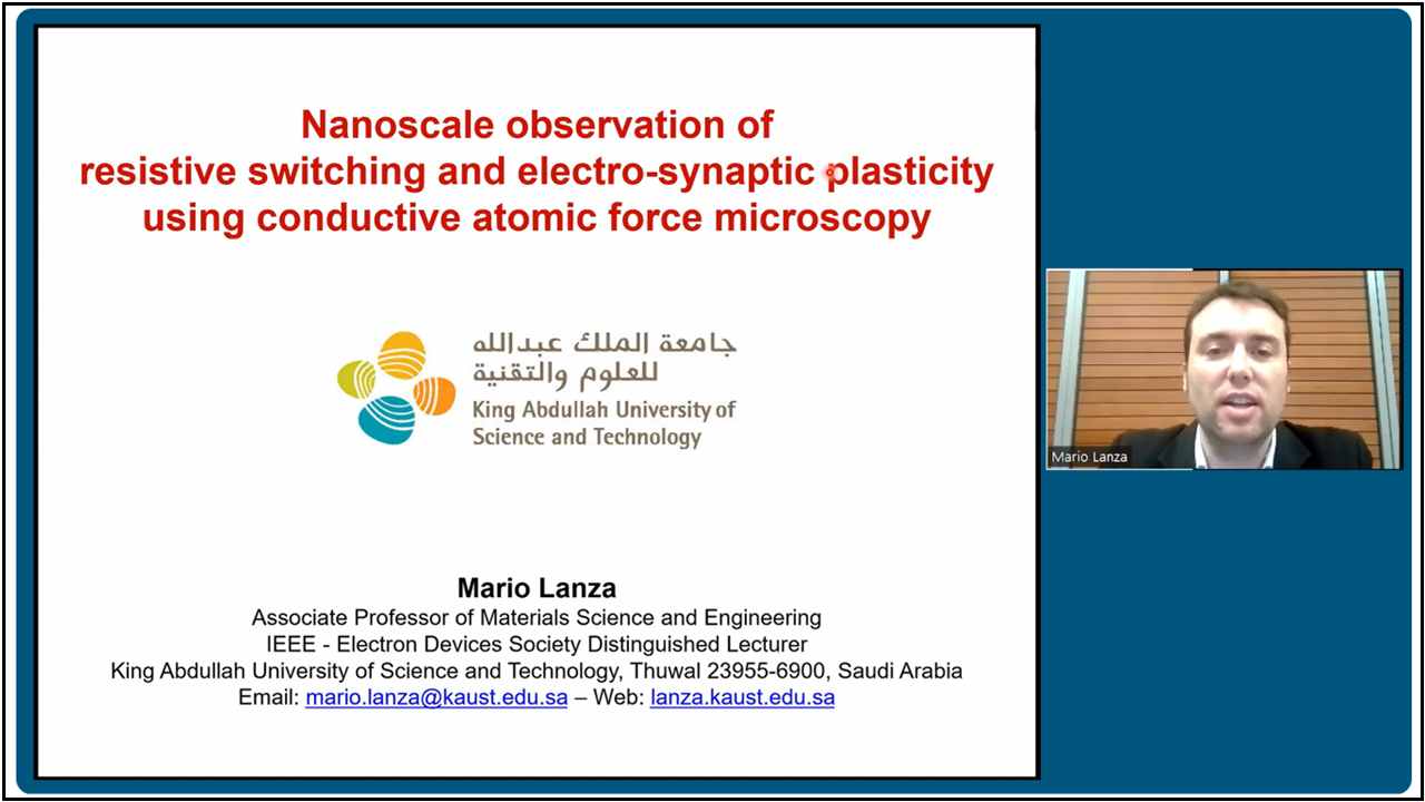
Conductive AFM
In this online seminar, Prof. Mario Lanza speaks about how to characterize the electronic properties of materials and devices at with nanometric precision using the conductive atomic force microscope (CAFM). This nanoelectronic metrology skill is for which Prof. Lanza was elevated to IEEE Fellow in 2024.
-
Interview CAFM inventor
In this video, Prof. Mario Lanza interviewed Dr. Sean O’Shea, who is one of the co-inventors of Conductive Atomic Force Microscopy. They discuss about how this invention happened and he gives practical advice to students and researchers working in this field, especially on how to reliably preserve tip quality.
-
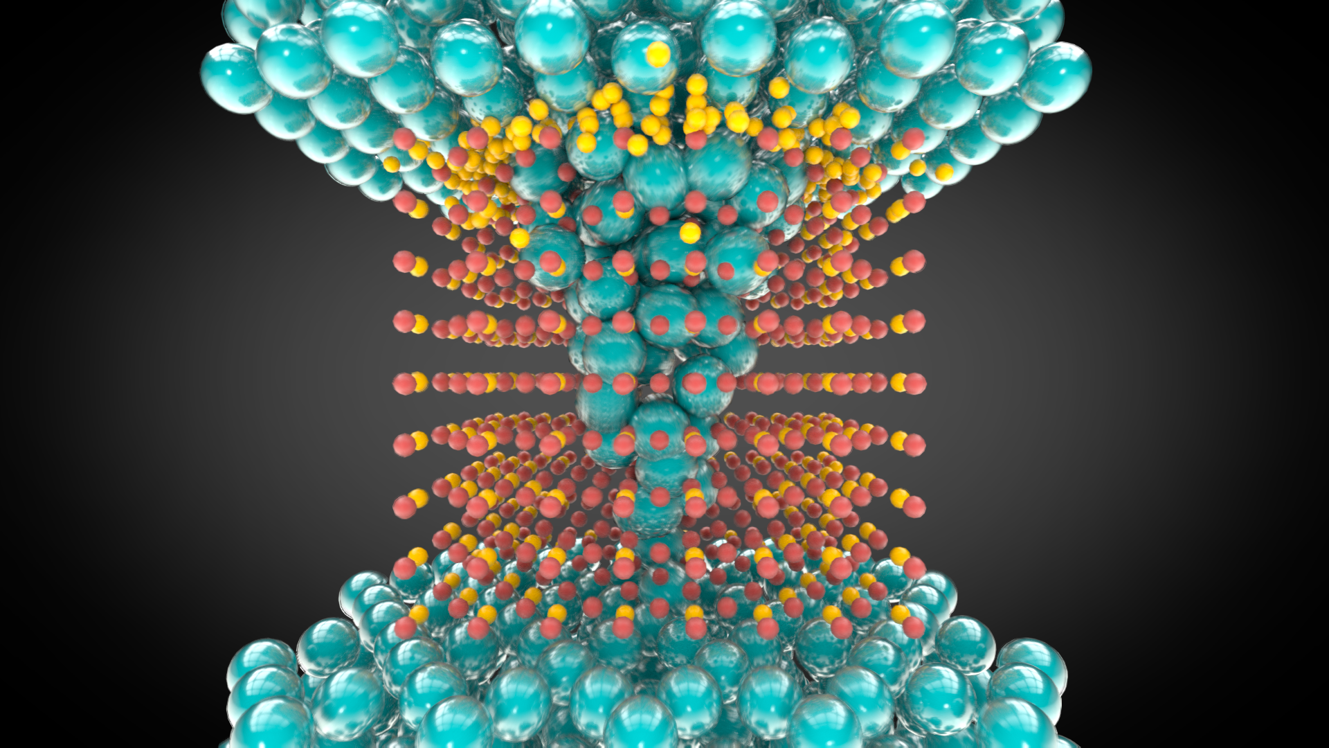
Animation
This animation was done to illustrate the concept idea and working mechanims of our memristors based on a 2D material called multilayer hexagonal boron nitride (hBN). The video presents the formation of a conductive nanofilament with metal ions difussing from the electrodes into the hBN stack.
Watch more videos in our Youtube channel: https://www.youtube.com/@lanzalab/videos